Lab 3: Keypad Scanner
Introduction
This report outlines the design and verification process for a 4x4 keypad matrix with TDM 7-segment display outputs
Design and Verification methodology
To make block level verification as simple as possible, I factored the design into three FSMs that each handle a small set of tasks, with handshakes between them where necessary.
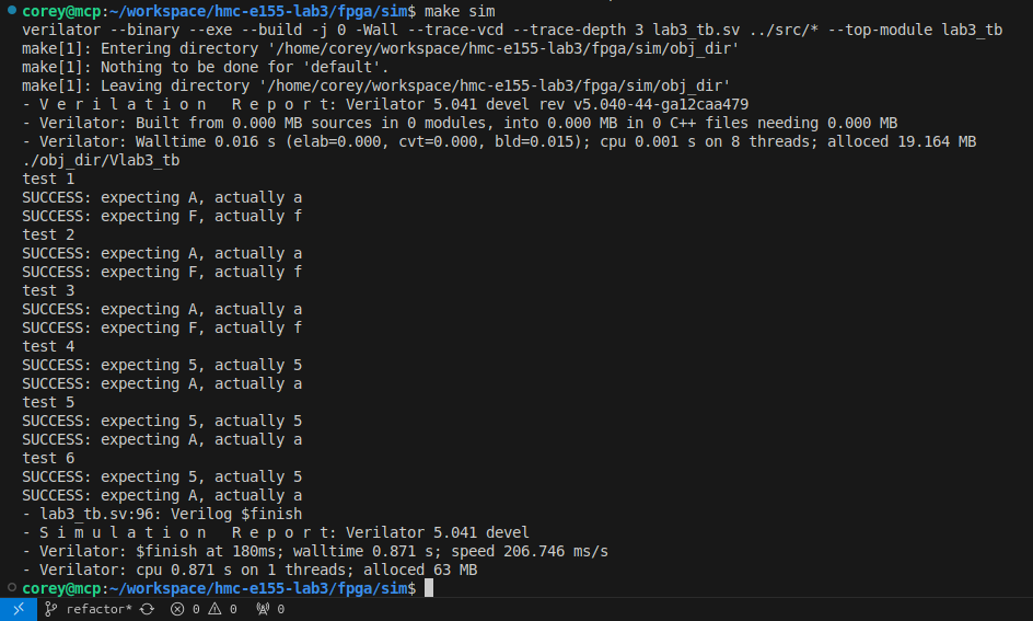
I did block formal verification for this project using SymbiYosys. With this tool, I proved that a set of design assertions were impossible to break for each major design element. For system level verification, I produces a simple simulation testbench to demonstrate the glue logic between the formally verified blocks.
Technical Documentation
The SystemVerilog source code for this lab can by found on my github page
Block Diagram
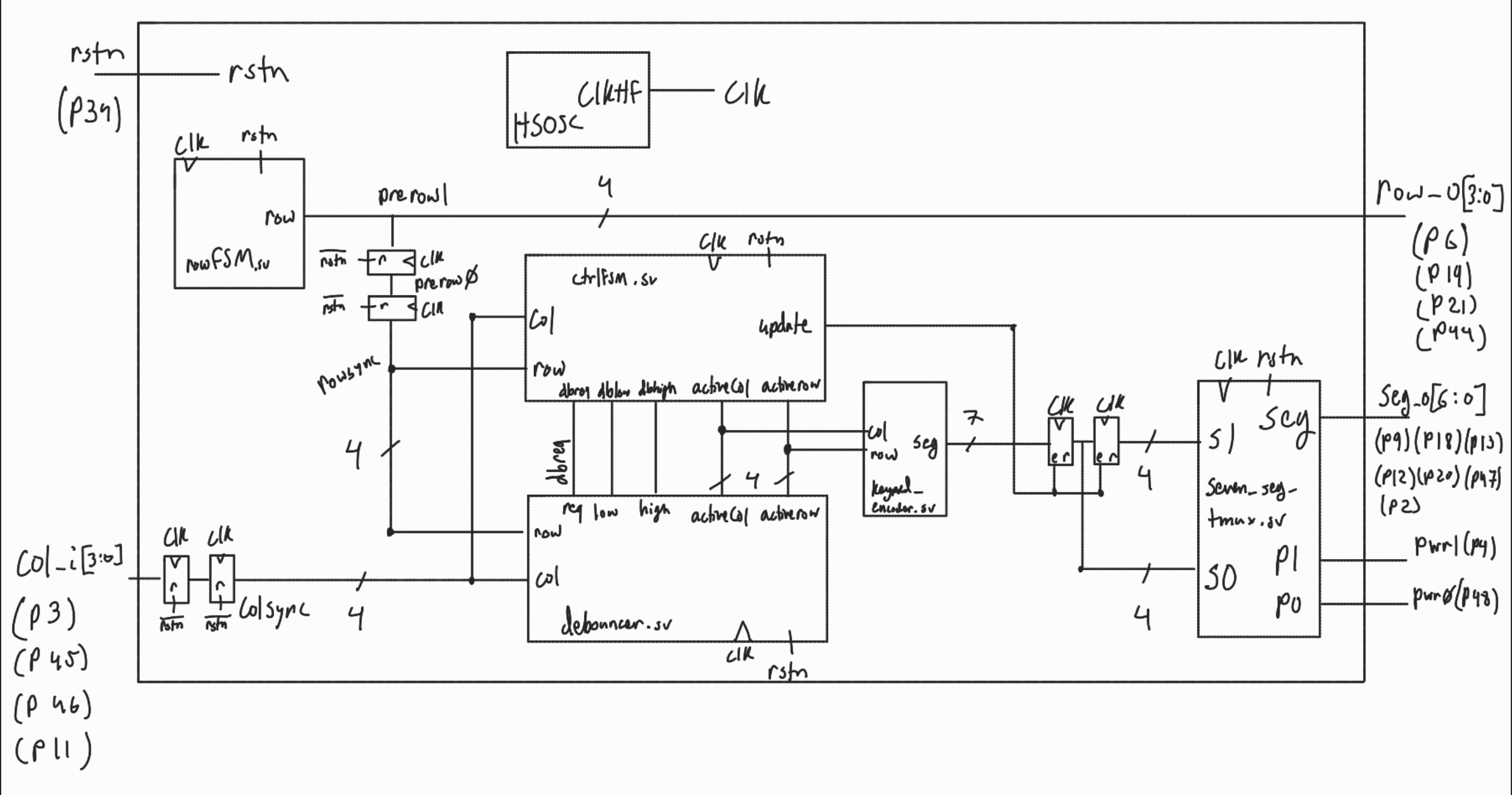
The block diagram in Figure 1 demonstrates the design structure with the three major FSMs, an encoder to convert row and column indecis into a hex value, and the time division multiplexer circuit derived from lab 2
State transition diagrams/tables
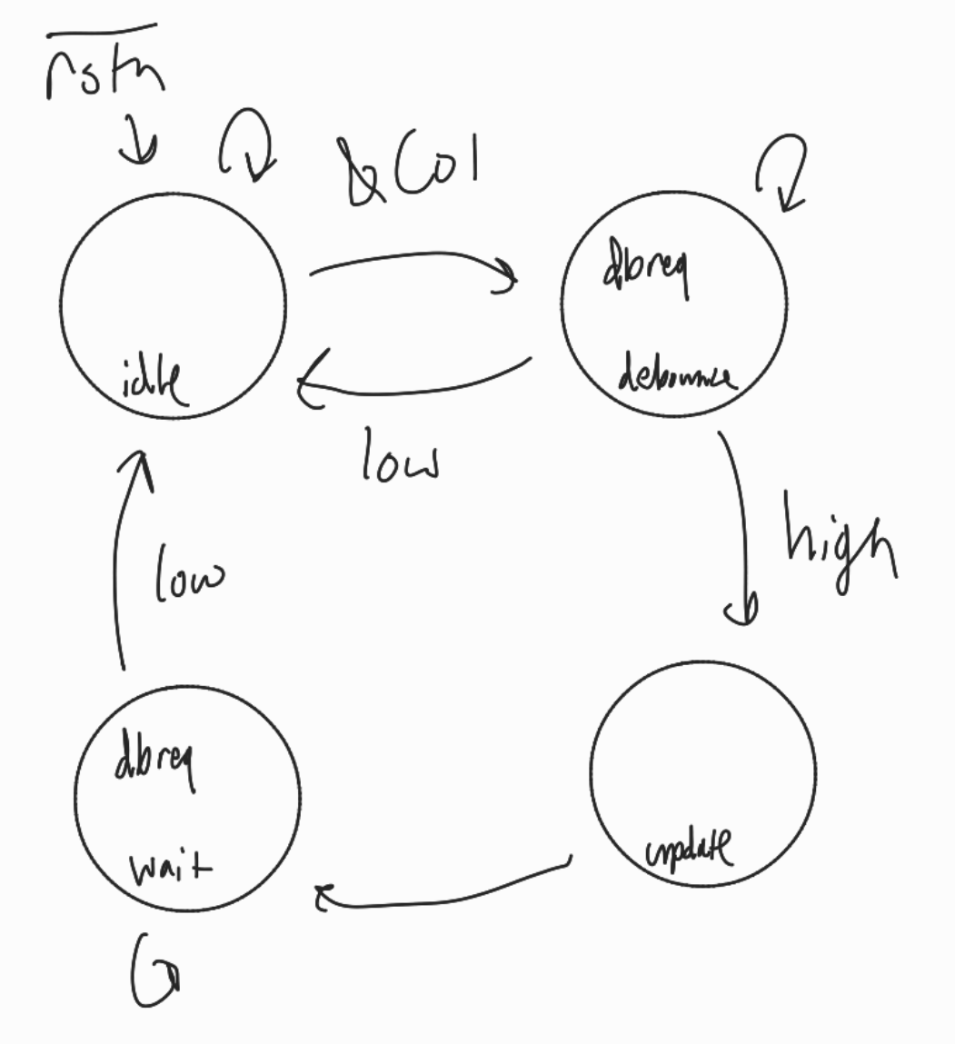
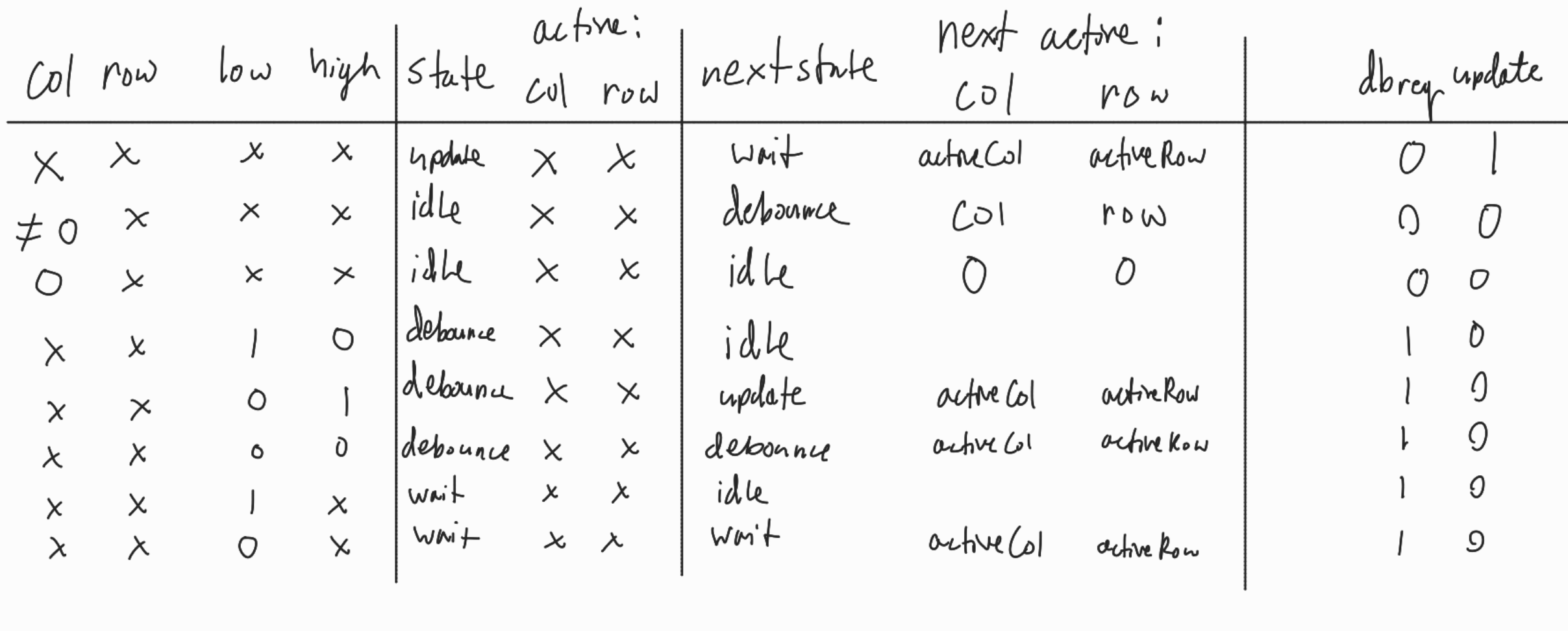
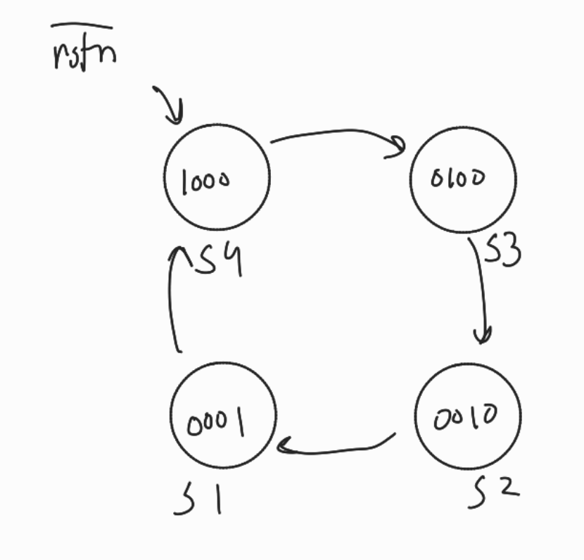
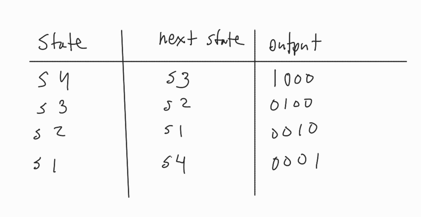
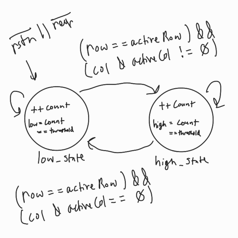
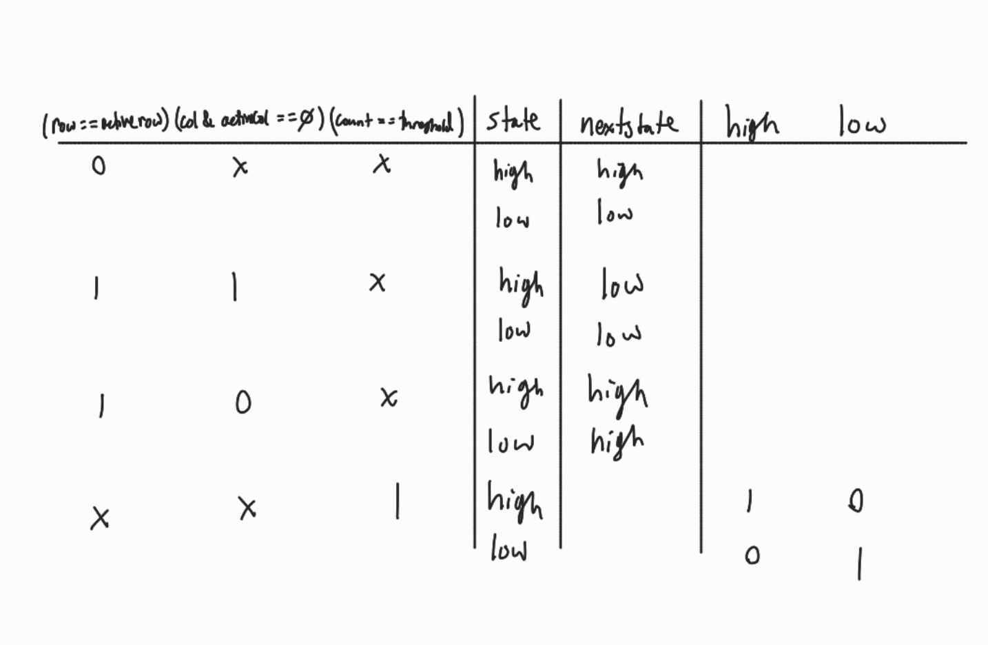
Figures 2-7 demonstrate the design of the three FSMs seen in the block diagram in figure 1
Schematic
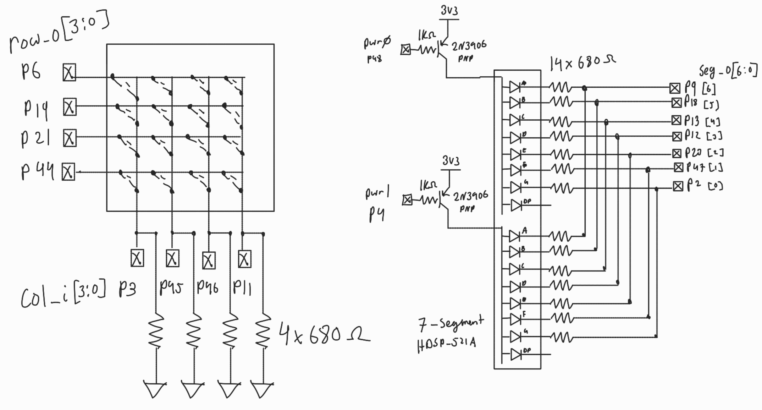
The schematic in Figure 8 demonstrates the phsyical hardware layout of the design, with the 4x4 keypad, 7-segment display, PNP transistors, pull down resistors, and current limiting resistors.
Component Values
For this lab we had 3 different resistor values to calculate.
First, we needed the current limiting resistors for the 7-segment LED arrays driven by the PNP resistors. For safety, I aimed for ~3 mA. Red LEDs have a voltage drop of ~1.8V and there is a voltage drop of ~0.2V between the collector and emitter of the PNP transister, per the datasheet, so we get the following calculation
\[ R = \frac{3.3V - 0.2V - 1.8V}{3mA} = 433 \Omega \]
Next, we have the resistor binding the base of the PNP transistor to the IO pin that powers each 7-segment display. Since the upper voltage is 3.3V going into a silicon diode that connects to the base, the voltage at the base is 0.7V lower or 2.6V. When the pin that is bridged to this terminal by a resistor is low, we wish to limit the current into the pin, so we aim for a large resistor. If we aim for around 3 mA of current, then we get the following equation for R:
\[ R = \frac{3.3V - 0.7V}{3mA} = 866 \Omega \]
To be extra safe and make use of readily available components, I used 680 Ohms for the current limiting resistors and 1 kOhms for the resistors connected to the PNPs.
Finally, for the external pull down resistors I chose 680 Ohms since this value would safely be low enough to prevent bringing the default pin voltage above the lower logic level. This likely could have been increased to save power, but since that wasn’t a particular concern, I chose this lower value to be safe.
Results and Discussion
Formal verification results
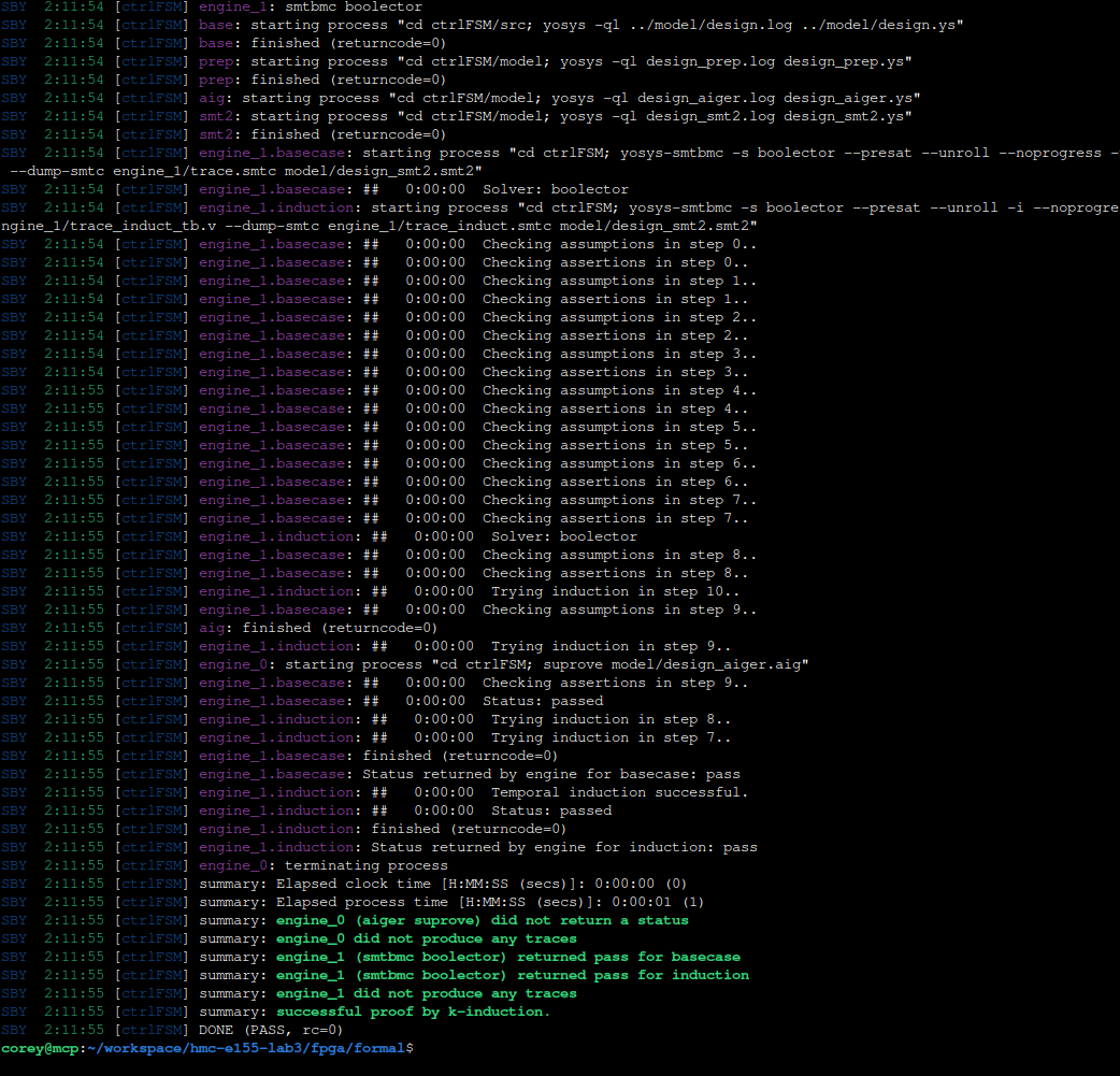
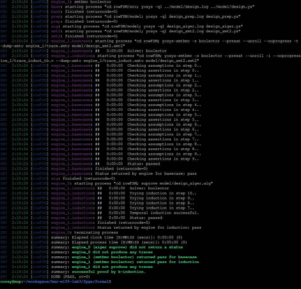
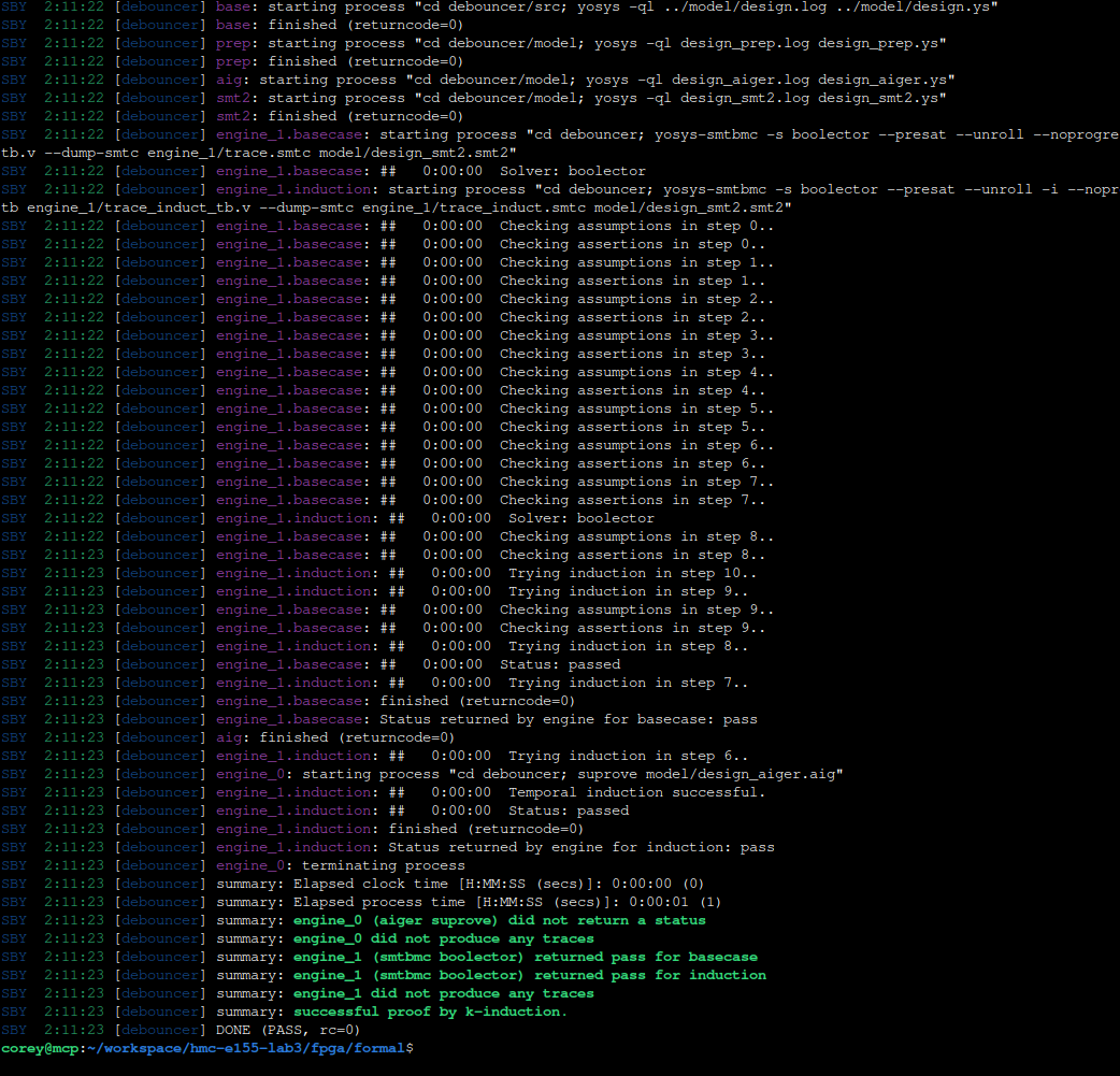
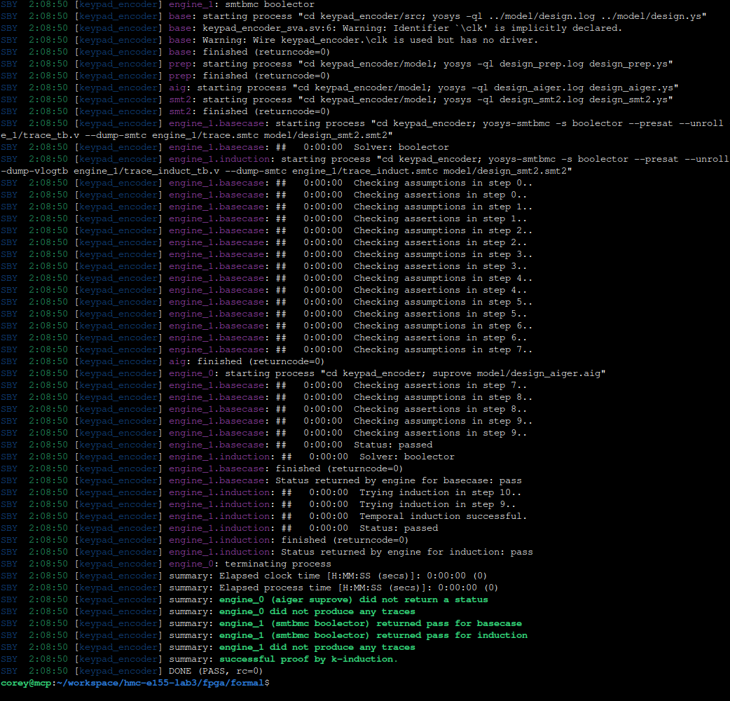
These formal verification results demonstrate that each major submodule adheres to a set of application specific design properties for all time, proving that they work as expected.
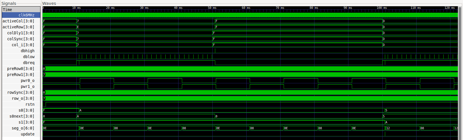
Hardware testing
Every button was checker for proper behavior. When one button was pressed, no other buttons affected the display. Additionally, I observed that the two segments did no flicker or bleed into one another, and were reletively bright.
Conclusion
I was able to design a matrix keypad driver circuit to read button presses from a real-world user. I brushed up on my synchronous design skills and my ability to formally describe the intended behavior of a sequential design without explicit test cases, as to be able to use formal verification.
I spent around 35 hours on this lab making sure my design meets all requirements
AI Prototype
First, I gave Microsoft Copilot the following prompt:
“Target device: Lattice iCE40 UP5K FPGA with internal high-speed oscillator (~20 MHz).
Write synthesizable SystemVerilog to scan a 4x4 matrix keypad and display the last two hex keys pressed on a dual 7‑segment display. Implement:
A clock divider that derives a scan clock on the order of 100–200 Hz from the internal oscillator. A keypad scanning controller that iterates one active‑low column at a time and samples active‑low rows, registering at most one key per press (debounce‑by‑design), ignoring additional presses while any key is held, and allowing a new registration only after release. A top level that updates two hex digits (older and most recent) when a new key is registered and drives a time‑multiplexed two‑digit 7‑segment display without visible flicker and with balanced brightness. Use idiomatic SystemVerilog (e.g., logic, always_ff, enumerated states for FSMs). Provide clean module boundaries and keep all state synchronous. Include brief comments explaining the design choices.”
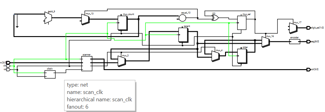
Initially, it did not synthesize due to the use of a $clog2 function call for a cute one-liner priority encoder. After pointing this out, it make a custom SystemVerilog function to perform this functionality. After this change, it synthesized with the following netlist viewer result:
Next, I gave this LLM the following three prompts back-to-back:
“Target device: Lattice iCE40 UP5K FPGA.
Overall Goal: Write SystemVerilog to scan a 4x4 matrix keypad and display the last two hex keys pressed on a dual 7 segment display.
Current Goal: Write a synthesizable SystemVerilog module that produces a one‑shot registration signal for the keypad system. Behavior:
When a key press is first detected, capture the current key code and assert a single‑cycle “new key” pulse. While any key remains pressed, do not accept additional keys. Only after keys are released should a subsequent press be recognized. This should handle debouncing of the keys. Implement as a small synchronous FSM with enumerated states and glitch‑free outputs. Keep names and interfaces reasonable; do not assume any hidden modules beyond what you define here.”
“Target device: Lattice iCE40 UP5K FPGA.
Write a synthesizable SystemVerilog module that cycles through keypad columns (active‑low, one at a time) and samples rows (active‑low) to detect a single key at a time. Behavior:
Iterate columns at a suitable scan rate derived from the divided clock and sample rows. When a key is detected, report a stable key code consistent with a standard 4x4 keypad layout and maintain it while the key remains pressed. Provide a boolean signal indicating whether any key is currently pressed. Use clean state encoding and synchronous logic; avoid combinational feedback and latches.”
“Target device: Lattice iCE40 UP5K FPGA with internal oscillator as the root clock source.
Write a top‑level SystemVerilog module that instantiates the scanner and one‑shot modules, shifts the last two keys (older ← most recent; most recent ← new), and drives a multiplexed two‑digit seven‑segment display. Requirements:
Update the displayed digits only when a new key is registered. Ensure equal apparent brightness and no visible flicker. Keep all logic synthesizable and synchronous; use idiomatic SystemVerilog constructs. Provide any small clock‑enable or divider logic you need. You can also assume that a sevenSegment module exists that takes a 4 bit input and outputs the 7 segments.”
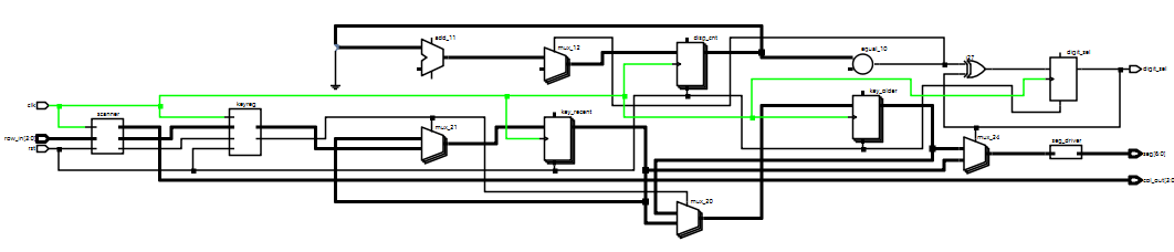
Again, it did not synthesize initially since it was missing a keypad encoder module. Once this was pointed out and corrected, I got the following:
These designs are prett similar to mine, but were done in a small fraction of the time. I would be curious to see how well they did on the physical hardware, as there are many subtle hardware edge cases that I am not sure the AI model is considering in producing this code.
Overall I am impressed with its performance, but I am also not shocked it missed synthesis issues and came up with nonstandard solutions.